
Key Takeaways
- 1If you bought five or fewer qualifying G.Skill kits, file with no documentation required at GSkillDRAMSettlement.com or by calling 877-755-4222.
- 2The payout is roughly $4.92 per product, and it will likely shrink further as more claimants file against the fixed $2.4 million pool.
- 3Only kits rated above 2133 MHz (DDR4) or 4800 MHz (DDR5) qualify; anything at or below those JEDEC defaults was never sold as an overclocked product.
- 4The claim window covers purchases from January 31, 2018 through January 7, 2026, with all claims due by April 7, 2026.
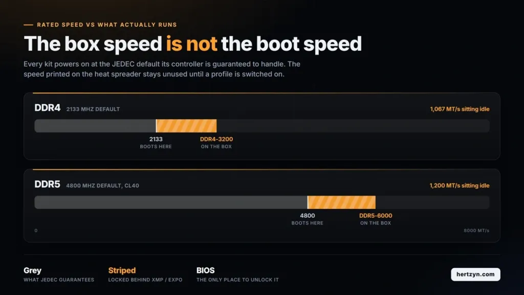
- 5A rated speed on the box does nothing until XMP or EXPO is enabled in BIOS; until then, every kit runs at its JEDEC default.
- 6CPU-Z reports DRAM frequency, not the transfer rate on the label; double a 1600 MHz reading to get DDR4-3200.
- 7With PC DRAM prices forecast to climb 105 to 110 percent in Q1 2026, tuning an existing kit’s profile is worth more right now than buying a faster one.
- 8The bigger long-term win isn’t the check, it’s the new ‘up to’ labeling requirement, which Igor’s Lab flagged as the outcome likely to outlast the payout itself.
G.Skill International Enterprise Co. Ltd. has agreed to a $2.4 million class action settlement, resolving a case brought by plaintiffs Hurd et al. in the U.S. District Court for the Central District of California. G.Skill has not admitted wrongdoing anywhere in the agreement, and the settlement itself does not establish that the underlying allegations are true, only that the company has chosen to pay rather than litigate them further.
- The suit alleges G.Skill advertised DDR4 kits at speeds above 2133 MHz without disclosing that this figure sits above what the memory runs at out of the box.
- It makes the same allegation for DDR5 kits advertised above 4800 MHz.
- In both cases, the complaint says G.Skill left out that a buyer has to go into BIOS and turn on XMP or EXPO themselves before the memory will run anywhere near the number on the box.
Who Qualifies: Speed Thresholds and Purchase Window
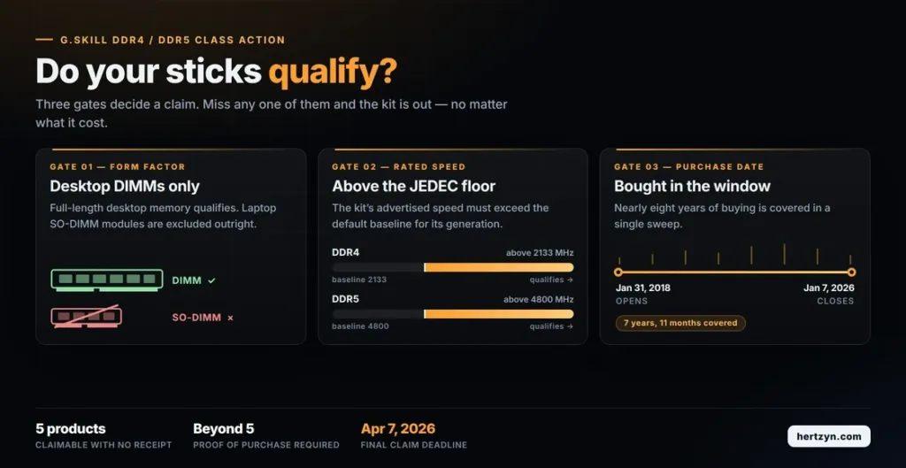
Three gates decide a claim. The stick has to be desktop memory, not a laptop SO-DIMM, and it has to carry a rated speed above the baseline: over 2133 MHz for DDR4, over 4800 MHz for DDR5. Those two cutoffs sit right at the ceiling of JEDEC’s own default clocks for each standard, which means anything running at or below them was never sold as anything but base-spec memory in the first place, and the settlement draws its line exactly where a marketed overclocking profile would have to start. The purchase itself then has to fall inside a window stretching from January 31, 2018 to January 7, 2026, nearly eight years of buying covered in one sweep.
Eligibility and Filing at a Glance
| Qualifying DDR4 speed | Exceeding 2133 MHz |
| Qualifying DDR5 speed | Exceeding 4800 MHz |
| Product type | Desktop memory only |
| Laptop SO-DIMM | Not included |
| Purchase window | January 31, 2018 through January 7, 2026 |
| Claim deadline | April 7, 2026 |
| Max claim without proof | 5 products |
| Proof required for more than five | Proof of purchase for each item beyond five |
| File claim at | GSkillDRAMSettlement.com |
| Administrator phone | 877-755-4222 |
How to File a Claim
Filing takes one of two forms: through GSkillDRAMSettlement.com or by calling the settlement administrator at 877-755-4222, with every claim due by April 7, 2026. Anyone claiming five qualifying products or fewer needs no documentation at all, which covers most builders who bought a kit or two over the years without keeping the receipt. Claim a sixth product or more, though, and the administrator wants proof of purchase for each one past that fifth, so anyone with a stack of kits from multiple builds should start digging through old order confirmations now rather than in April.
First Payments: About $4.92 Per Product
Recipients started reporting electronic payments landing on August 18, 2026, the first hard evidence that the settlement had moved from paperwork to actual money.
The figures people are posting line up cleanly: $4.92, $9.84, $19.68, and $24.60, which map to one, two, four, and five approved products respectively. That arithmetic only works if every product is being valued the same way, which is exactly what lets us back out a per-unit number nobody officially stated.
| Reported payment (USD) | Approved products |
|---|---|
| 4.92 | 1 |
| 9.84 | 2 |
| 19.68 | 4 |
| 24.60 | 5 |
Not an Official Figure
The settlement administrator hasn’t published a per-unit rate anywhere. $4.92 is what it looks like once you line up enough recipient reports and see the same number repeat, not a figure anyone at the fund has confirmed.
Final approval came down in June 2026, roughly two months before the first payments started showing up, which is about the lag you’d expect for an administrator to process claims and cut checks after a settlement clears court.
Why the Per-Product Rate Can Still Move
$4.92 isn’t a rate anyone set going in. Court-approved fees come out of the $2.4 million fund first, and whatever’s left gets split across every valid claim, so the number only exists once the claims window closes and the total count is known. That means the payout per product moves in one direction as more people file: the more claimants, the smaller each one’s check.
JEDEC Baseline Speeds for DDR4 and DDR5
Every stick of desktop memory, regardless of what’s printed on the heat spreader, boots up at a JEDEC default speed the module and the motherboard’s memory controller are both guaranteed to handle without any tuning. For DDR4 that number is 2133 MHz. For DDR5 it’s 4800 MHz, or in some cases 5600 MHz, run at a JEDEC latency of CL40. JEDEC sets these numbers conservatively on purpose: they’re the speed a board and a stick from unrelated manufacturers can be plugged together and expected to just work, which is the entire point of having a standard at all.
| DDR4 JEDEC default speed | 2133 MHz |
| DDR5 JEDEC default speed | 4800 MHz, sometimes 5600 MHz |
| DDR5 JEDEC latency | CL40 |
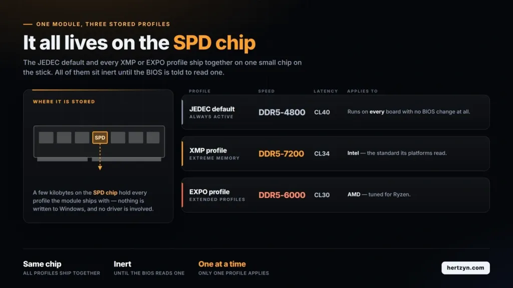
| XMP profile standard | Intel |
| EXPO profile standard | AMD, optimized for Ryzen |
| Profile storage location | RAM SPD chip |
XMP and EXPO: Getting Past the Default
XMP is Intel’s overclocking profile standard, and EXPO is AMD’s equivalent, optimized for Ryzen. Both work the same way: the higher speed printed on the box, the one the settlement’s thresholds are actually measured against, is written to a small SPD chip on the module alongside the JEDEC default, and it sits there doing nothing until the BIOS is told to read it. Enabling XMP or EXPO in BIOS is what applies that stored speed along with its timings and voltage; skip that step and the memory runs at JEDEC default no matter what’s on the label.
Enabling and Verifying the Profile
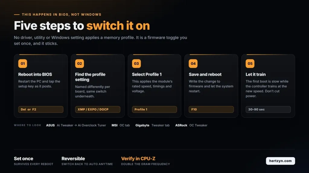
- ASUS: under Ai Tweaker, then Ai Overclock Tuner
- MSI: under the OC tab
- Gigabyte: under the Tweaker tab
- ASRock: under OC Tweaker
- Restart the PC and press Delete or F2 to enter BIOS.
- Find the XMP, EXPO, or DOCP setting in the menu.
- Select Profile 1 to apply the module’s rated speed.
- Press F10 to save changes and reboot.
- Let the first boot run its course; it can take 30 to 90 seconds as the system trains at the new speed.
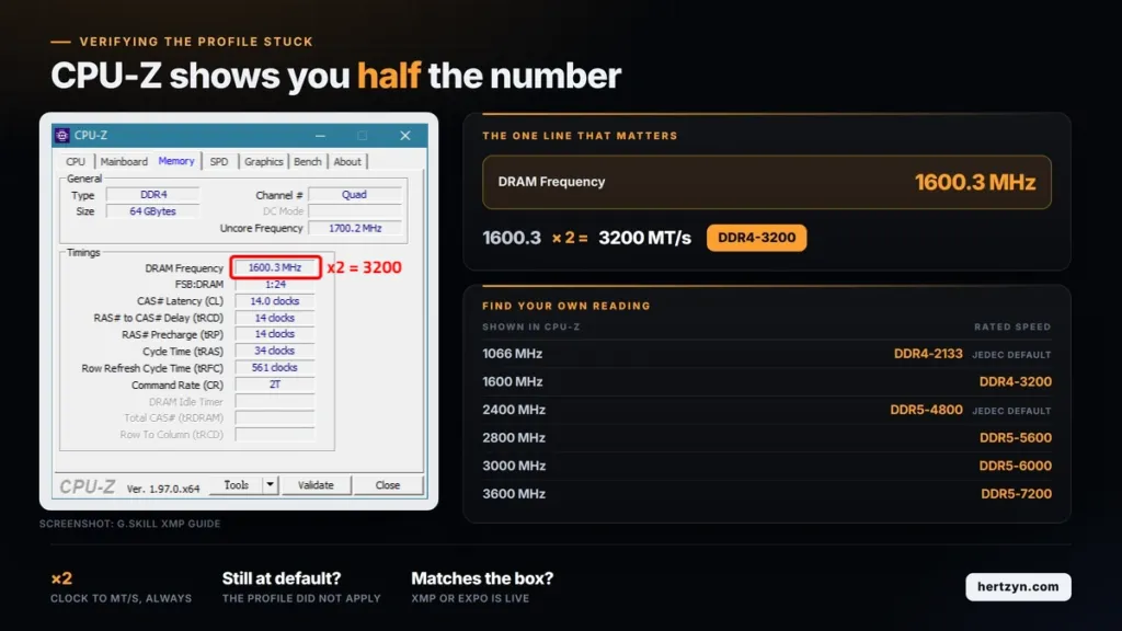
CPU-Z’s Memory tab reports the DRAM frequency, not the transfer rate on the box, and the two aren’t the same number. DDR memory transfers data twice per clock cycle, so a CPU-Z reading of 1600 MHz corresponds to DDR4-3200; the number on screen has to be doubled to get the MT/s figure a rated speed is actually sold on.
AM5 and Intel: Different Sweet Spots
PC DRAM prices are forecast to jump 105 to 110 percent in Q1 2026, which changes the math on this settlement entirely. Getting an existing kit stable at a higher profile is worth more right now than shopping for a faster one, since the faster one is about to cost dramatically more than it does today.
| Platform | Sweet spot | Profile | Why this speed |
|---|---|---|---|
| AMD AM5 (Ryzen 7000/9000) | DDR5-6000 CL30 | EXPO | IMC runs 1:1 up to ~6000-6200; beyond that drops to 2:1 and latency rises |
| Intel LGA1700 (14th gen) | DDR5-7200 CL34 | XMP | IMC operates in Gear 2, decoupled from memory speed; higher MT/s is genuinely faster |
CUDIMM is an Intel Z890 story
CUDIMM’s onboard clock driver only does its job on Intel Z890 boards. Drop the same module into an AMD X870E or X870 board and the clock driver runs in bypass mode, doing nothing, so a Ryzen buyer paying the CUDIMM premium is paying for a feature that never switches on.

Slot count matters as much as the kit itself. Four DIMMs loaded onto a board add electrical load and signal reflections that two don’t, which is why every motherboard’s QVL lists a lower maximum speed for a four-stick configuration than for a two-stick one. Two higher-density sticks will almost always clock higher than four smaller ones chasing the same total capacity.
The memory controller itself is subject to silicon lottery, not just the RAM. Two identical Ryzen 9 9950X chips can land at DDR5-6400 on one sample and DDR5-5800 on another, even running the same kit. Most AM5 chips handle DDR5-6000 EXPO without complaint, and 70 to 80 percent go on to hit 6400, but if a given CPU won’t hit the kit’s rated speed the fix is dropping the profile or setting it manually slower rather than assuming the memory is at fault.
AM5 boards retrain their memory settings from scratch on every cold boot unless Memory Context Restore is enabled, which saves the trained configuration instead of redoing the work each time. For the fastest possible boot, pair Memory Context Restore with Power Down Enable.
RAM manufacturers have advertised XMP and EXPO profiles as if they were guaranteed clock speeds for as long as those standards have existed, and this settlement is one of the first times that habit has cost a company money. Every kit on the market ships with a rated speed printed in bold on the box, achieved only after a buyer enables a profile in BIOS, and until now nobody had been made to answer for the gap between that number and what a stick does at stock.
New Labeling Requirements Under the Settlement
- Advertised speeds must be presented as ‘up to’ figures rather than flat numbers
- Packaging must disclose that overclocking or BIOS adjustments may be required to reach the rated speed
- Packaging must note that maximum performance depends on the CPU, motherboard, and other system components
Igor’s Lab put the payout in blunt terms: about $4.92 per product funds little more than lunch, and nobody filed a claim expecting it to cover the cost of a kit, let alone the premium paid for a higher-rated one. Whatever this settlement is worth to a buyer, it isn’t the check.
Igor’s Lab found the labeling change the more interesting outcome of the two. A marketing style that’s gone unquestioned since XMP launched now carries a specific disclosure requirement, at least for one manufacturer, and that outlasts any $4.92 check landing in an inbox. Whether other vendors adopt the same ‘up to’ language voluntarily, or wait for their own lawsuit, is the part of this settlement worth watching next year rather than this one.